 |
| Digital Audio |
| NEW! Dual Zo Digital Audio |
| Custom & HV |
| Catalog |
| FAQ's |
| RoHS Lead Free FAQ |
| Latest News |
| About Us |
| Contacts |
| 1998 AES Paper |
| 2001 AES Paper |
| 2003 AES Paper |
| Sales |

| The Effects and Reduction of Common-Mode Noise and Electromagnetic Interference in High-Resolution Digital Audio Transmission
Presented at the Audio Engineering Society Convention, New York October 2003 By Jon D. Paul, Vice President |
|
|
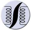
ABSTRACT High-resolution digital audio systems are especially susceptible to sources of electromagnetic noise from the environment, for example, crosstalk from adjacent cables. The noise can induce errors and increase jitter in the recovered clock signal. We discuss the most important noise sources and their characteristics. Next, we analyze the noise susceptibility of typical transmitter and receiver circuits. Test results are provided for a system with induced common-mode noise. The paper concludes with circuit design, component and application considerations. Transmitter Common-Mode Noise/EMI Current Paths
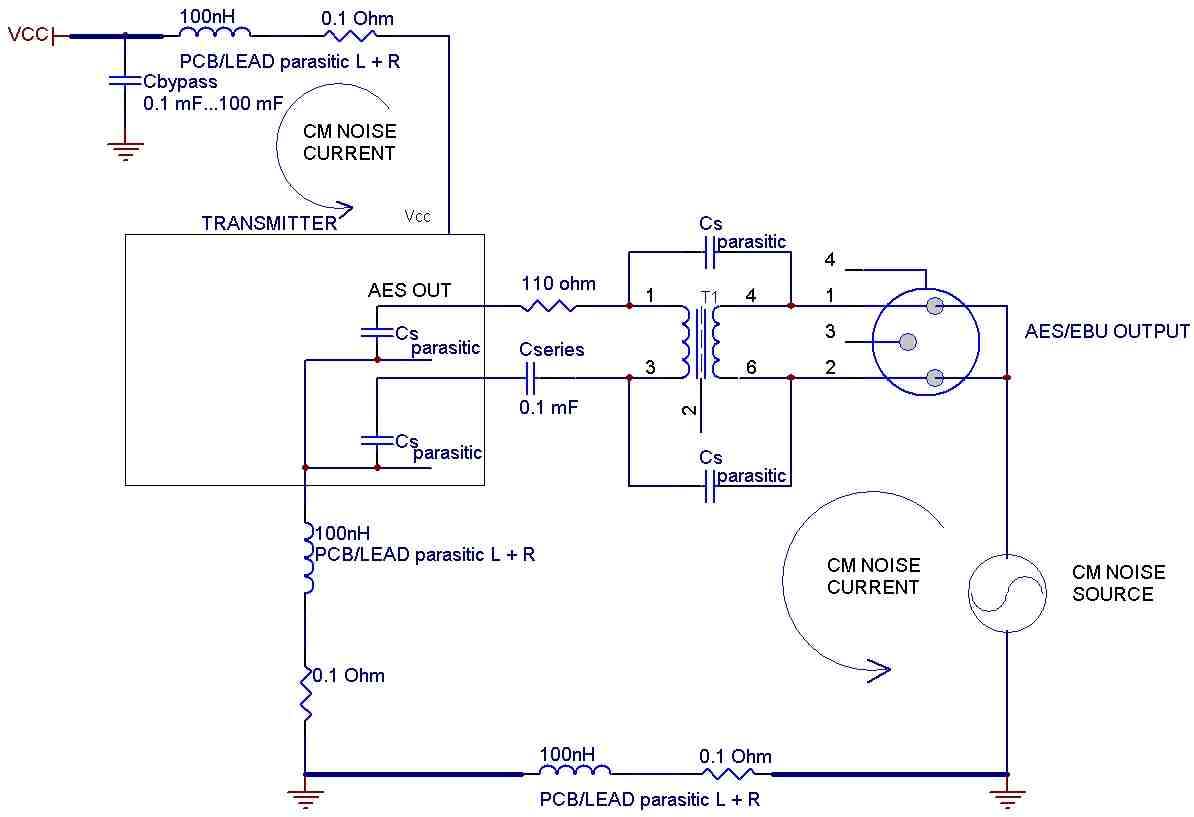
Simulation Results: CMRR vs. Frequency
without transformer, 15 pF Cp-s and 0.5 pF Cp-s transformer
High Capacitance vs. Low Capacitance Transformers
30 dB CMRR difference at 10 MHz!
Improved
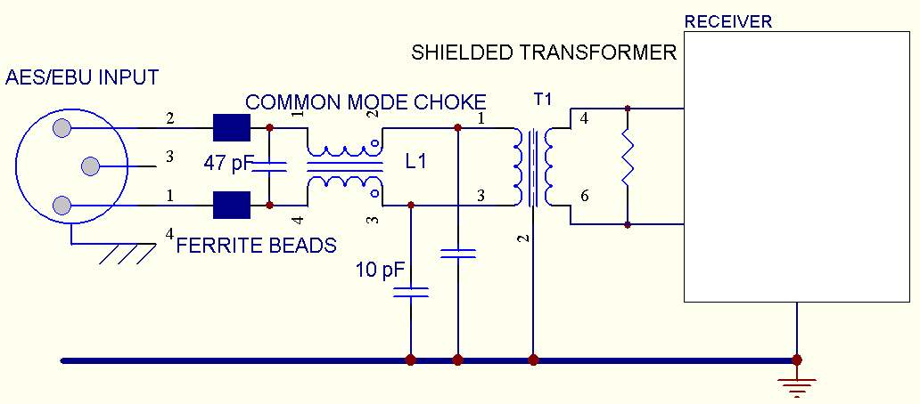
Receiver Circuit: Beads, CM Choke and Shielded Transformer
|
|
|
Figures Fig. 1 Unbalanced Transmission System Fig. 2 Balanced Transmission System Fig. 3 Balanced Transmission System with Noise Sources Fig. 4 Normal-Mode and Common-Mode Currents Fig. 5 Resistive Coupled Interference (“ground loop”) Fig. 6 Capacitive (Electric) Coupled Interference
Fig. 7 Inductive (magnetic) Coupled Interference Fig. 8 Common-Mode to Differential-Mode Conversion Fig. 9 RS-485 Output Driver and IC Manufacturer’s Suggested Circuits Fig. 10 Transmitter Common-Mode Noise/EMI Current Paths Fig. 11 RX IC Manufacturer’s Suggested Circuits Fig. 12 RX and RS-485 Input Circuit, Transfer Function Fig. 13 Balanced RX Common-Mode Noise Current Fig. 14 Receiver with Reclocking Stage Common-Mode Noise Current Paths Fig. 15 Simulation Model: Common-mode Gain of Transformer + Diff Amp. Fig. 16 Transformer and Differential Amp Simulation of CMRR vs. Frequency Fig. 17 RX Differential Signal Eye Pattern with Common-mode Noise Fig. 18 Common-mode Interference Test Fixture Fig. 19 RMS Jitter and Histogram Test Equipment Fig. 20 Common Mode Noise at TX Fig. 21 RX Inputs With CM Interference Fig. 22 TX IC Power CM current Hi Cap Trsf X vs. Shielded Low Cap Trsf S2 Fig. 23 RX Induced Jitter No Transformer Jitter 1.505 ns RMS Fig. 24 RX Induced Jitter Transformer X Jitter 3.104 ns RMS Fig. 25 RX Induced Jitter TX Transformer Y, Jitter 7.83 ns RMS Fig. 26 RX Induced Jitter Low Capacitance Transformer S1, Jitter 297 ps RMS Fig. 27 TX Induced Jitter No Transformer Jitter 19.367 ns RMS Fig. 28 TX Induced Jitter Hi Capacitance Transformer X, Jitter 84.5 ns RMS Fig. 29 TX Induced Jitter Lo Capacitance Transformer S1, Jitter 1.64 ns RMS Fig. 30 TX Induced Jitter Shielded Transformer S2, Jitter 302 ps RMS Fig. 31 Jitter Histogram Interpretations Fig. 32 Jitter Histogram Interpretations Fig. 33 Reclocking RX with Transformer Isolation Fig. 34 Balanced Transmission System Using Shielded Transformers Fig. 35 Application of Transformers to Unbalanced System Fig. 36 Transformer Parameter Comparison Fig. 37 Transformer Construction Fig. 38 Improved Receiver Circuit with Shield Beads, Choke & Transformer Fig. 39 Common-mode Chokes Fig. 40 Suggested PCB Groundplane for Transformer & Receiver Fig. 41 Double Termination Fig. 42 Double Termination vs. Secondary Termination Reflection Coefficient Summary and Conclusions
The circuitry of a high-resolution digital audio interface is especially sensitive to common-mode noise, crosstalk and electromagnetic interference. The design of interface circuits and printed circuit board layouts must consider this interference susceptibility to realize high quality, low jitter transmission of digital audio signals.
New product designs should be tested for interference susceptibility to detect and debug the effects of noise and interference on clock jitter and data errors. |
|
|
NOTE: If the papers don't load completely, save the PDF file to your disk; open with Acrobat Reader 7. Copyright © 2008 Scientific Conversion, Inc. All rights reserved. Information is subject to change without notice.
Last revised: |
|

All material on this website is Copyrighted, use without permission is prohibited.